The latest trend in technology is converting all wired interfaces to wireless. Whether it is in Consumer, Automotive, Medical, or Industrial Industry. This conversion of interfaces from wired to wireless gives more flexibility, convenience and provides world-wide access instead of the area bound wired access. According to the new market research report, it is expected that the market will reach to 8.78 billion units by 2023 from 6.51 billion units in 2018, at a CAGR of 6.2% between 2018 and 2023.
Building hardware products itself is a time-consuming and costly process. Whereas designing wireless products requires proper antenna type-specification selection, placement, and precautions to meet RF measurements as expected. Failing to do so will increase the time-to-market, development cost and drastically may require multiple spins. Adding this to the latest IoT application requires the product to be more compact with multiple RF solutions embedded into it, which will hold the complexity of RF and product design to the next level and add loads of risks in product design.
Working on the conventional antenna performance measurements on an actual prototype can solve the purpose to some extent, where there is a limited number of (one or two) RF antenna and low complexity in the product. Having multiple antennas in small form factor, high complexity and specific RF performance criteria in a product not follow this approach. As in many cases, the selected RF antenna solution doesn’t work as expected, which may reduce time to market and increases the development cost.
To tackle this hurdle, where designers seek to optimize the product design process and development cost considering the RF solution complexity. RF simulation is a solution that can remove this extra burden of risks.
RF simulation is colossal, growing with considering its simulation complexity and methods. There is multiple simulator software like HFSS, CST, ADS, etc. which should be wisely used according to the problem type. Mostly HFSS is selected for RF antenna design/simulation for embedded solutions. Designers require to effectively integrate this RF antenna simulation in their product design methodology, approaches, and validation phases to get the maximum benefits. The need for product designs is becoming more and more complex, where product designers/managers are confused about, how effectively add RF antenna design in product-hardware development stages. The new simulation details and data requires new techniques for product design management.
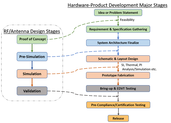
Fundamentally, RF antenna design/simulation verifies product options and also helps to choose the correct action as the product evolves through the design cycle. Therefore, the link between the hardware product design and RF antenna design shows, how the RF design stages must be included in product development cycle stages.

Proof of Concept
Proof of Concept(POC) stage starts from the basic idea of a product without any mechanical model in place. The required details are product use-cases, antenna requirements, estimated PCB sizes, major metal parts (if any), material details and desired product size. Simulation is carried out using simplified mechanical models, which will provide details on the feasible and non-feasible algorithm. Later on, the major blocker can be identified in this stage only, which will help the product owners to create better business cases and product specifications.
Pre-simulation
After completion of the POC stage, the hardware requirement specification and system architecture are finalized. The pre-simulation is accomplished with the latest/ more-rich model designed by mechanical engineers. This phase may require multiple iterations until the antenna solution is concluded. Additionally, this phase will also provide minimum distance, location, and orientation of different antenna solutions in multiple antenna products. The phase should ensure that the remaining changes in the product should not affect the RF antenna solution. The pre-simulation phase is the major in overall RF antenna simulation stages.
Simulation
Once the schematic and layout design is completed, the simulation or virtual testing stage begins. By this time, the mechanical enclosure will also be finalized for the prototype. Therefore, this simulation is carried out on the full-featured/extremely detailed mechanical model. Exact enclosure, mechanical part properties, and material details are required, to get the exact details which will help to have more accurate RF simulation results. Further, it requires to optimize the RF performance, and test possible effects of nearby mechanicals, metal, and PCB layout changes. Here, the accuracy of RF simulation depends on accurate and well-defined details which help to get the possible risk in the final product and be prepared in advance.
Validation
The validation stage starts, once the prototype boards are ready and bring-up testing is completed. Even though simulation claims high accuracies, but it always needed to validate the simulation results with physical measurements. It is also required to rule out the human error and provided the simulation details correct. Additional incorporated filters during the pre-simulation & simulation stage will require to tune for optimum performance in the validation stage. The validation stage of RF antenna measurements will be filled in the remaining gap of RF antenna product design.

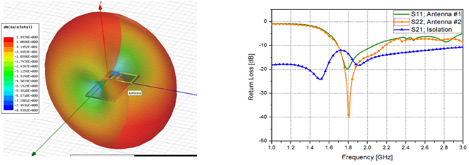
During this complete RF antenna simulation design stages, there are multiple parameters that are considered and assured that the design/simulation RF antenna solution meets their requirements. The parameters are antenna type, antenna placement, orientation, antenna isolation when multiple antennas are in design, return loss, VSWR, gain, bandwidth, radiation efficiency, effects of the ground plan, effects of nearby parts on radiation patterns.
Integrating the RF antenna design/simulation in hardware products as above would help to design complex RF antenna products in an effective way. It reduces the RF risk gradually, right from the starting requirement stage to avoid major blockers for a product in later stages. The product owners can take proactive decisions based on simulation results instead of actually hitting the risk.
About VOLANSYS
VOLANSYS has been diligently involved in offering Product Engineering, Digital Engineering and Quality Engineering from conceptualization to manufacturing. Our product development strategy is to meet the evolving market demands at the same time ensuring consumer satisfaction, critical timelines, and budgets. We have devised out energy-efficient manufacturing techniques and charted out a formidable low time to market plan, leading to a successful market hold for our clients.
Note: The content of this blog is based on the personal knowledge of any research work done by any individuals. There is a market research report on wired interfaces that is used from websites Wired Interface Market. Figures are kept with the best of our knowledge and not to mislead by any manner.

About the Author: Bimal Makwana
Bimal Makwana works with VOLANSYS Technologies as Principal Engineer and looks after Embedded Hardware Design and end to end solutioning. Bimal has a rich experience of around 7+ years in various domains of product development which includes from product concept, system architecture design to final certification that brings greater value to our clients to implement a one-stop solution.


