Contact Us
VISIT US: USA
2890 Zanker Road, Suite 200, San Jose, CA – 95134
MAIL US:
[email protected] (Inquiry)
CALL US 24/7:
+1 510 358 4310

Latest Blogs

  • Break The Connectivity Barriers with Wi-Fi 7
  • Intelligent Health Environment
  • AI-Driven Quality Engineering
  • Complete Guide to Develop a Home Automation App
  • Machine to Machine Communications
  • Safe RTOS

VOL NXP i.MX7ULP uSOM

Overview

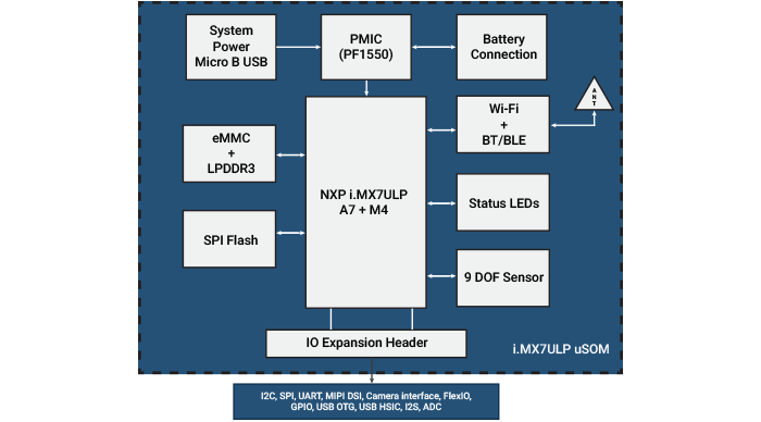
The VOL NXP i.MX7ULP uSOM is an ultra-low-power processor SOM featuring heterogeneous multi-core processing architecture with an Arm® Cortex®-A7 core which operates at 800MHz, paired with an Arm® Cortex®-M4 core which operates at 200MHz. It also has 3D and 2D Graphics Processing Units (GPUs), 32-bit LPDDR2/LPDDR3 external memory, flash memory, and supports interfaces like MIPI DSI display, parallel camera, I2C, SAI, UART, SPI, USB, etc. The Cortex® A7 core supports Android & Linux operating systems whereas the Cortex® M4 core supports FreeRTOS. It is a highly integrated multi-market applications processor designed to enable ultra-low-power and secure, wearable applications. Targeted towards the growing market for portable devices, it is best suited for use cases demanding long battery life and high-end graphics.

Key Features

  • Heterogeneous multi-core processing architecture
  • 2D and 3D Graphics Processing Units (GPU)
  • External memory support: LPDDR2/LPDDR3
  • Flash memory support: managed NAND (eMMC, eSD)
  • MIPI DSI display interface
  • Parallel camera interface
  • 512KB of total SRAM
  • Quad SPI (w/ On The Fly Decryption)

Key Applications

  • Smart Home Controls
  • Power & Energy Management Systems
  • Industrial Control Systems
  • Consumer Electronics
  • Healthcare
  • Wearables
  • Building Automation
  • Portable scanners and printers

Technical Specifications

ProcessorNXP i.MX7ULP
TechnologyHeterogeneous multi-core processing architecture
with application domain and real-time domain
  • ARM® Cortex®-A7
    Nominal frequency: 500 MHz Overdrive: 800MHz (Application Domain)
  • ARM® Cortex®-M4
    Maximum frequency: 200 MHz (Real Time Domain)

Graphics Processing Unit

  • Integrates GPU for 2D graphic composition processing with GC320 and supports user interface rendering and performs functions
  • Integrates the GC7000 Nano Ultra GPU supporting OpenGL ES2.0/1.1, desktop OpenGL 2.1, OpenVG 1.1, and GLSL shading language support.
Feature VersionWith GPU
Without GPU
OS SupportA7: Linux and Android
M4: FreeRTOS
PowerUSB Power Supply Range: DC 4.1V – 6V (Typical – 5V)
Current requirement – 600mA maximum
Battery input: 3.7V DC (Rechargeable battery), supports up to 1.0A battery charging current
LPDDR3 DRAM1GB
eMMC8GB
QSPI Flash64MB
EEPROM 4KB
 Interface with application domainInterface with real-time domain
USB
  • 1x interface, USB OTG 2.0 modules with integrated USB PHYs
  • 1x interface, integrated USB 2.0 PHY capable of connecting to USB host/device systems
  • 1x interface, integrated USB 2.0 PHY capable of connecting to USB host/device systems
  • 1x interface, integrated USB 2.0 HSIC Phy connectivity interface
QSPI1x interface, single data rate/ double data rate mode of operation at 108 MHz in STR mode with 4-bits, 80 MHz for DDR mode without DQS with 4-bit and 100 MHz for DDR mode with DQS 8-bit
SPI 2x interface, synchronous serial interface with clock configurable to 60 MHz master/ 30 MHz slave modes max.2x interface, synchronous serial interface with clock configurable to 30 MHz master/ 15 MHz slave modes max.
I2C4x interface, supporting high speed with data rate up to 1 Mbps, configurable as master/ slave modes
SAI2x interface, full duplex serial interfaces with frame synchronization, such as I2S, AC97, and codec/DSP interfaces
MIPI DSI Display2 lanes MIPI DSI interface, supported up to 800Mbps data rate on each lane
Parallel Camera1x interface, up to 24-bits and supports maximum pixclock of 66.7MHz and resolution from Supports QVGA to 1080P input resolution
ADC2x interface, 12-bits general purpose analog to digital converter
JTAG1x interface, production, testing and debugging with JTAG TAP standard
Flex IO1x interface, 32-bits dFlex IO is supporting wide range protocols like UART, I2C, SPI, I2S, camera
interface, display interface
Wi-FiWi-Fi – 802.11 b/g/n
BLEBT + BLE 4.1
AntennaOn-board RF antenna
9DOF3-axis Gyroscope
3-axis Magnetometer
3-axis Accelerometer
eFusesYes
RNGYes
Secure RTCYes
Encrypt/decrypt enginesYes
Tamper DetectionYes
Secure BootYes
DimensionsL x W x H – 32 mm x 28 mm x 4.5 mm
Operating TemperatureCommercial: 0 to + 70 °C
Industrial: -40 to + 85 °C
RoHSCompliant
CEWork in progress
ICWork in progress
FCCWork in progress
Processor NXP i.MX7ULP
Technology Heterogeneous multi-core processing architecture with application domain and real-time domain
  • ARM® Cortex®-A7 Nominal frequency: 500 MHz Overdrive: 800MHz (Application Domain)
  • ARM® Cortex®-M4 Maximum frequency: 200 MHz (Real Time Domain)
Graphics Processing Unit
  • Integrates GPU for 2D graphic composition processing with GC320 and supports user interface rendering and performs functions
  • Integrates the GC7000 Nano Ultra GPU supporting OpenGL ES2.0/1.1, desktop OpenGL 2.1, OpenVG 1.1, and GLSL shading language support.
Feature Version With GPU
Without GPU
OS Support A7: Linux and Android
M4: FreeRTOS
Power USB Power Supply Range: DC 4.1V - 6V (Typical - 5V)
Current requirement - 600mA maximum
Battery input: 3.7V DC (Rechargeable battery), supports up to 1.0A battery charging current
LPDDR3 DRAM 1GB
eMMC 8GB
QSPI Flash 64MB
EEPROM  4KB
  Interface with application domain Interface with real-time domain
USB
  • 1x interface, USB OTG 2.0 modules with integrated USB PHYs
  • 1x interface, integrated USB 2.0 PHY capable of connecting to USB host/device systems
  • 1x interface, integrated USB 2.0 PHY capable of connecting to USB host/device systems
  • 1x interface, integrated USB 2.0 HSIC Phy connectivity interface
-
QSPI - 1x interface, single data rate/ double data rate mode of operation at 108 MHz in STR mode with 4-bits, 80 MHz for DDR mode without DQS with 4-bit and 100 MHz for DDR mode with DQS 8-bit
SPI  2x interface, synchronous serial interface with clock configurable to 60 MHz master/ 30 MHz slave modes max. 2x interface, synchronous serial interface with clock configurable to 30 MHz master/ 15 MHz slave modes max.
I2C 4x interface, supporting high speed with data rate up to 1 Mbps, configurable as master/ slave modes -
SAI - 2x interface, full duplex serial interfaces with frame synchronization, such as I2S, AC97, and codec/DSP interfaces
MIPI DSI Display 2 lanes MIPI DSI interface, supported up to 800Mbps data rate on each lane -
Parallel Camera 1x interface, up to 24-bits and supports maximum pixclock of 66.7MHz and resolution from Supports QVGA to 1080P input resolution -
ADC 2x interface, 12-bits general purpose analog to digital converter -
JTAG 1x interface, production, testing and debugging with JTAG TAP standard -
Flex IO 1x interface, 32-bits dFlex IO is supporting wide range protocols like UART, I2C, SPI, I2S, camera interface, display interface -
Wi-Fi Wi-Fi - 802.11 b/g/n
BLE BT + BLE 4.1
Antenna On-board RF antenna
9DOF 3-axis Gyroscope
3-axis Magnetometer
3-axis Accelerometer
eFuses Yes
RNG Yes
Secure RTC Yes
Encrypt/decrypt engines Yes
Tamper Detection Yes
Secure Boot Yes
Dimensions L x W x H – 32 mm x 28 mm x 4.5 mm
Operating Temperature Commercial: 0 to + 70 °C
Industrial: -40 to + 85 °C
RoHS Compliant
CE Work in progress
IC Work in progress
FCC Work in progress

Hardware Design

VOLANSYS-iMX7ULP-uSOM-Hardware-Design

Don’t hesitate to contact us any time

Our experts can help you accelerate your digital transformation journey!